

On May 25, 2026, at IEEE ISCAS 2026, He Tingbo, President of Huawei's Semiconductor Business Unit, introduced a key concept: the τ Law. τ, the time constant in circuit theory, determines the speed at which a signal transitions from one state to another. This marks the first time a Chinese company has proposed a new principle guiding industry development in the global semiconductor field.
More concretely, over the past six years, Huawei has mass-produced 381 chips based on this law, covering core scenarios such as wireless base stations, AI inference, and network processors . This is not a blueprint, but a proven path. It is projected that by 2031, high-end chips based on the τ law will reach an equivalent 1.4nm process level, maintaining the ability to compete with international mainstream technologies in the long term.
Today, this Greek letter is quietly changing the value landscape of the semiconductor industry and bringing EDA from behind the scenes to the forefront.
To understand what τ will bring to the EDA industry, we must first understand what the τ law actually is.
"Time shrinkage" has just made its debut, so what makes the τ law so important?
Moore's Law, proposed by Intel co-founder Gordon Moore in 1965, states that the number of transistors that can be placed on an integrated circuit roughly doubles every 18 to 24 months, while performance improves and costs decrease.
For over half a century, this logic has been working effectively, supporting PCs, the internet, smartphones, and now artificial intelligence. The industry chain has also developed a tacit understanding around it—lithography machines, materials, and design, each link is advancing collaboratively on the path of miniaturization. However, around 2000, there were dozens of wafer fabs capable of keeping up with the most advanced processes, but by 2025, that number had plummeted to just TSMC, Samsung, and Intel, with TSMC even quoting over $30,000 for a single 2nm wafer.
It's fair to say that the benefits of Moore's Law are gradually fading. The industry has explored multiple technological paths, including Nvidia CEO Jensen Huang's "Huang's Law," the International Technology Roadmap for Semiconductors (ITRS)'s "More than Moore" approach, and the Chiplet and advanced packaging technologies promoted by AMD and TSMC. Huang's Law emphasizes doubling the AI inference performance of a single GPU chip annually, but it still relies on process iterations and core stacking, essentially continuing the approach of geometric miniaturization. "More than Moore" adds value through the integration of analog/RF/sensor functions, but it cannot directly solve the digital logic latency wall problem. While Chiplet alleviates yield and cost issues by "building blocks," it introduces significant inter-die interconnect latency, which may become a bottleneck in some latency-sensitive scenarios.
Most of these solutions still follow the approach of "geometric miniaturization" or functional superposition, which is fundamentally different from the τ law.
The core of the τ law is "time minimization" instead of "geometric minimization," and it is a complete optimization system that spans four levels: devices, circuits, chips, and systems. It is suitable for large-scale system-level performance improvements, and it is particularly advantageous in AI and heterogeneous computing scenarios.
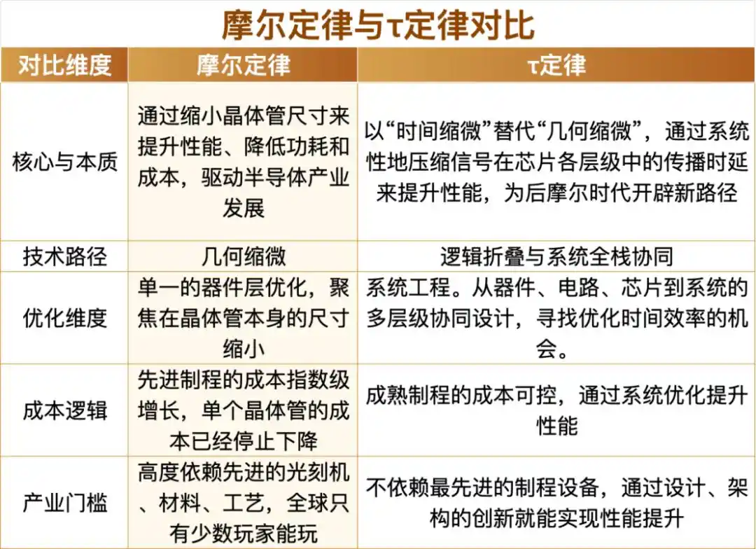
He Tingbo explained in detail that at the device level, by optimizing transistors, interconnect resistances, and parasitic capacitances, the device-level time constant τ is minimized to the maximum extent from the physical level. At the circuit level, logic folding technology breaks through the physical boundaries of traditional planar layouts, significantly shortening the trace length of critical paths and effectively reducing the resistance and capacitance load of signal propagation, thereby achieving a significant improvement in transistor density and circuit performance. At the chip level, through a full-stack hardware-software co-design of "software, architecture, and chip," fine-grained control of instruction and data flows is achieved based on actual workloads, improving system-level parallelism and efficiency, and significantly reducing end-to-end execution time. At the system level, the Lingqu bus is defined, the computing system interconnection protocol is reconstructed, and unified memory addressing and native memory semantics of supernodes are achieved, significantly reducing system communication latency.
In comparison, T-law aligns more closely with the core essence of chip computing power: the core function of a chip is information processing, and end users are more concerned with the latency of information processing than the number of transistors and the size of the manufacturing process. This law provides a new technological route for chip design that moves beyond simple process miniaturization, meaning that it is possible to create chip products with satisfactory overall performance without using top-tier lithography equipment. Therefore, it does not contradict Moore's Law; the two are compatible. It can be understood as: Moore's Law is about continuously drawing finer grids on a plane, while T-law is about folding the paper, using three-dimensional space to obtain shorter signal paths.
It is worth noting that every step of the implementation of the τ law relies on a key player—EDA (Electronic Design Automation). It is no longer a "drawing tool" in the traditional sense, but has become the central nervous system for "time miniaturization" from theory to physical chip.
Huawei's paper reveals that its technological roadmap employs a coexisting approach combining three technologies: Chiplet advanced packaging, 3D integrated circuits (3DIC), and Logic Folding. This allows for optimized reorganization at different granularities in vertical integration. Achieving a more than 100-fold increase in hardware integration by 2035 presents three major challenges: the discontinuation of the EDA toolchain, cross-wafer process deviations, and the law of energy conservation.
Andrew B. Kahng, a distinguished professor of computer science and engineering and electrical and computer engineering at the University of California, San Diego, also stated that these fundamental goals in EDA and physical design will become even more important as the tailwinds brought by the traditional Moore's Law gradually diminish.
Therefore, EDA was placed back in the center of the table.
What new requirements does τ's law impose on EDA?
In response to the new requirements that the τ law places on EDA tools, as well as the existing shortcomings of traditional EDA tools, the author exchanged and discussed these issues with industry practitioners.
Firstly, the lack of native true 3D design and cross-layer collaborative optimization capabilities highlights the importance of STCO.
First, Peking University stated that the traditional 2D design process, and even the current mainstream "pseudo-3D" process—that is, after synthesis, each module is "pinned" to a certain die at once, and then implemented piece by piece using 2D EDA tools—cannot achieve flexible cross-layer allocation at the unit level.
Native 3D EDA tools integrate multiple dies into a unified 3D design space, supporting the free arrangement of standard units across dies. They also enable cross-die logic reconstruction and global optimization, providing crucial support for logic folding technology from design concept to physical implementation.
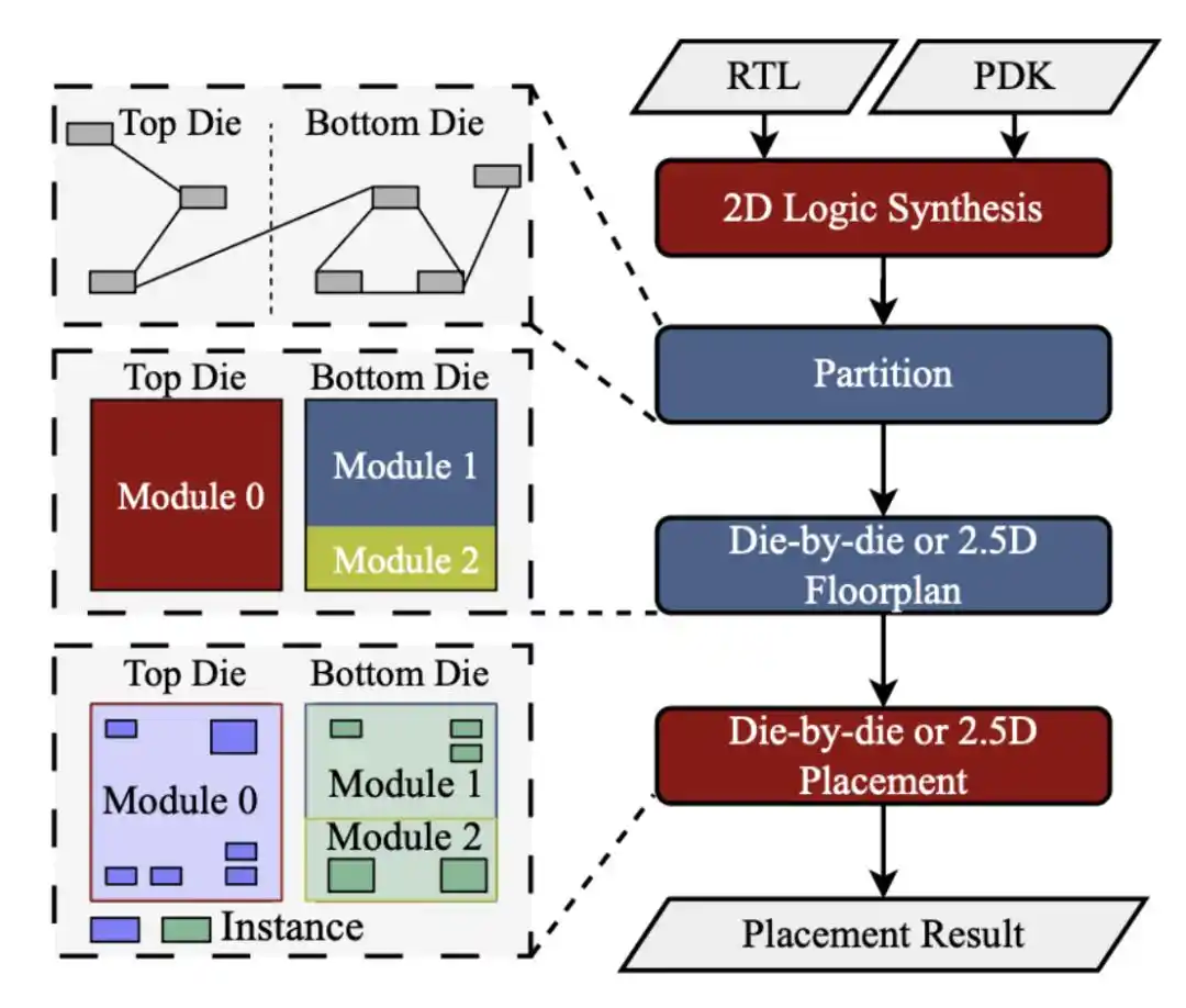
"Pseudo-3D" workflow vs. "True-3D" workflow. Source: Peking University
Furthermore, cross-layer collaborative optimization capabilities are also insufficient. Chiplet, 3DIC, and LogicFolding are implementations at different granularities along the same vertical integration line, according to Chiplet, 3DIC, and LogicFolding, as explained by Chiplets to Semiconductor Industry Insights.
Chiplet combines heterogeneous dies in 2.5D or 3D at the packaging level, using interconnect standards such as UCIe to move communication that was originally within a single SoC to between dies, trading modularity for yield and flexibility; 3DIC further introduces high-density TSVs and hybrid bonding between dies, vertically stacking logic, memory, and analog functions in the same package, compressing interconnect distances from millimeters to micrometers; LogicFolding goes a step further—it does not establish interconnects between dies, but rather vertically splits and redistributes the "internal logic of a single chip itself" at the active layer dimension, allowing the hybrid bonding interface to directly participate in the timing optimization of the critical path like an additional metal layer.
These three elements are not substitutes, but rather coexist and overlap in advanced packaging systems. This overlap presents a fundamental design engineering challenge: when a package simultaneously involves inter-chip UCIe interconnects, 3D interlayer hybrid bonding, and on-chip LogicFolding critical path folding, the analytical boundaries for signal integrity, power integrity, thermal distribution, and mechanical stress can no longer be closed individually at any single level.
The concept of STCO (System Technology Collaborative Optimization) was proposed precisely to break down this disconnect at the methodological level. It requires treating logical architecture, physical layout, multiphysics, encapsulation structure, and even workload as a unified design space, and conducting joint optimization searches across disciplines and abstract levels. This capability is precisely what is currently lacking at the lowest level of the EDA toolchain.
Secondly, there is a lack of multiphysics coupling.
This is one of the most hidden yet critical weaknesses of traditional EDA tools. In the era of single-chip solutions, power supply analysis, thermal simulation, and stress calculation belonged to multiple independent toolchains, each with its own modeling, solving, and approval processes. However, this model is no longer entirely applicable in three-dimensional stacked architectures. With the vertical integration of multiple bare dies, power density increases exponentially, heat dissipation paths become highly asymmetrical, and interlayer temperature differences increase. The resulting thermal expansion mismatch is conducted layer by layer in the stacked structure through microbumps and hybrid bonding interfaces, which not only deviates the electrical characteristics of the device but also introduces potential mechanical reliability risks.
What capabilities do EDA vendors need to improve?
Currently, most domestic EDA companies focus on single-point breakthroughs, tackling challenges in their respective niche areas of expertise. From simulation to physical verification, from yield improvement to layout design, a number of outstanding domestic EDA companies have developed usable and competitive point tools in many aspects.
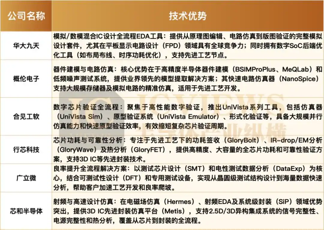
For example, Huada Jiutian is one of the earliest companies in China to engage in EDA R&D. Based on analog EDA, Huada Jiutian has gradually expanded into digital and advanced packaging fields, committed to building a complete toolchain. Gailun Electronics takes a "bottom-level penetration" approach; it doesn't directly handle the entire process, but focuses on device modeling and circuit simulation. Hejian Software is a leading digital EDA company in China, representing a full-process/platform model. Xingxin Technology chooses to focus on the most difficult "approval" stage. Xinhe Semiconductor focuses on "advanced packaging." Guangli Microelectronics emphasizes yield improvement and is the only company capable of forming a complete closed loop through "equipment data acquisition + software data analysis."
The τ law is expected to drive the domestic EDA industry to upgrade from "localization of point tools" to an industrial software foundation that is " full-process, cross-level, and highly collaborative ." This means that the EDA toolchain will no longer just undertake auxiliary functions such as circuit drawing, layout design, and back-end verification, but will need to be fully embedded in key processes across the entire chain, including device modeling, PDK construction, circuit simulation, parasitic parameter extraction, timing and power analysis, physical verification, advanced packaging, and system-level collaborative optimization.
On May 26, the School of Integrated Circuits at Peking University announced a key breakthrough in its prototype "True 3D" EDA tool, developed to address the logic folding requirements of Tao's Theory. This tool supports complete 3D spatial collaborative optimization, cross-die logic free allocation and joint thermal optimization, and can cover tens of millions of instance designs. Compared to traditional "pseudo-3D," Peking University's "True 3D" EDA achieves: an average reduction in line length of approximately 30%; an improvement in WNS of approximately 6% and TNS of approximately 12%; and a reduction in peak temperature of over 3%. The tool has already completed industrial-grade design verification and will be expanded to multi-die stacking and heterogeneous integration scenarios in the future, filling a crucial gap in 3D chip design.
On the same day, an investor asked Huada Jiutian on an interactive platform: In the post-Moore's Law era, the industry believes that the importance of EDA is evolving from a traditional design tool to a "system-level performance optimization platform." How does the company view the strategic value of EDA in logic folding, timing optimization, and multi-chip collaboration in the future?
Huada Jiutian subsequently responded: The company has a forward-looking insight into how AI, GPU, and storage chips are leveraging 3DIC technology to overcome the bottlenecks in advanced processes and computing power in the post-Moore's Law era. It has proactively positioned itself in the 3DIC design EDA field, building a complete solution covering the entire process from heterogeneous integrated 3D chip collaborative design to verification, filling the gap in high-end 3DIC design tools in China. It is the only domestic provider of full-process 3DIC design and verification EDA. The company launched its first industry-leading Argus 3DIC physical verification platform, fully supporting 2.5D/3D heterogeneous integrated packaging design, enabling full-link physical verification from diversified 3DIC collaborative design to packaging.
Thus, a path has gradually become clear, from the theoretical guidance of the τ law to the definition of system architecture, and then to the filling of gaps in domestic EDA toolchains. In the next few years, vendors that take the lead in launching industrially validated closed-loop solutions in areas such as timing convergence of logic folding, 3D multiphysics coupling signature, and STCO full-stack collaboration are expected to occupy a more proactive position in the trend of "time shrinking." For domestic EDA, this may provide a window of opportunity to shift from catching up with point tools to building full-stack capabilities—no longer just satisfied with "usability," but continuously evolving towards full-stack "ease of use."
This article is from the WeChat Official Account "Semiconductor Industry Insights" (ID: ICViews), author: Feng Ning

