
Original Title: ZPU: The Zero-Knowledge Processing Unit
Original Author: Ingonyama
Original source: medium
Compilation: Kate, Marsbit
TL;DR:
In this blog, we present the Zero-Knowledge Processing Unit (ZPU), a general-purpose programmable hardware accelerator designed to address the new demands of zero-knowledge processing.
We describe the ZPU architecture and design considerations. We explain the design choices behind different parts of the ZPU ecosystem: ISA, data flow, memory and processing element (PE) internals. Finally, we compare ZK and fully homomorphic encryption (FHE) with state-of-the-art ASIC architectures.
introduce
The rapid growth of data-driven applications and growing need for privacy has led to a surge in interest in encryption protocols that protect sensitive information. Among these protocols, Zero-knowledge Proof(ZKP) stand out as a powerful tool for ensuring computational integrity and privacy. ZKPs enable one party to prove the validity of a claim to another party without revealing any additional information. This property has led to the widespread adoption of ZKPs in various privacy-focused applications, including blockchain technology, secure cloud computing solutions, and verifiable outsourcing services.
However, adopting ZKPs in practical applications faces a major challenge: the performance overhead associated with proof generation. ZKP algorithms typically involve complex mathematical operations on very large integers, such as large polynomial computations and multiscalar multiplications on elliptic curves. Additionally, cryptographic algorithms are constantly evolving, and new and more efficient schemes are being developed rapidly. As a result, existing hardware accelerators struggle to keep up with the wide variety of cryptographic primitives and ever-changing cryptographic algorithms.
In this blog, we present the Zero-Knowledge Processing Unit (ZPU), a novel multi-purpose hardware accelerator designed to address the novel needs of zero-knowledge processing. The ZPU is built on an instruction set architecture (ISA) that supports programmability, enabling it to adapt to rapidly evolving encryption algorithms. The ZPU has an interconnected network of processing elements (PEs) with native support for large-word modular algorithms. The core structure of the PE is inspired by the multiply-accumulate (MAC) engine, a fundamental processing element in digital signal processing (DSP) and other computing systems. The operators of PE use a modular algorithm, and its core components are specially designed to support common operations in the ZK algorithm, such as NTT butterfly operation and elliptic curve point addition for multiscalar multiplication.
instruction set architecture
The ZPU architecture is characterized by an interconnected network of processing elements (PEs) defined by an instruction set architecture (ISA), as shown in Figure 1 below. We chose this architecture to adapt to the changing environment of zero-knowledge protocols.
The ISA approach enables the ZPU to remain flexible, adapt to changes in the ZK algorithm, and support a wide range of cryptographic primitives. Additionally, using an ISA rather than fixed hardware allows for continuous software improvement after manufacture, ensuring that the ZPU remains relevant and efficient even as new advances emerge in the field.
The ISA is a set of instructions that a processor can execute. It acts as an interface between hardware and software, defining the way software interacts with hardware. By customizing the ISA to design the ZPU, we can optimize it for the specific requirements of ZK processing tasks, such as large font arithmetic operations, elliptic curve encryption, and other complex cryptographic operations.
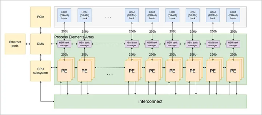
Figure 1: PE network structure
PE core components
Each PE has designed a core, including modular multipliers, adders and subtractors, as shown in Figure 2. These core components are inspired by the fundamental processing element of digital signal processing (DSP) and other computing systems, the multiply-accumulate (MAC) engine. The MAC engine efficiently performs a multiply-accumulate operation, which involves multiplying two numbers and adding the product to the accumulator.
The core structure of PE is tailored for common operations in ZK, such as elliptic curve point addition for multiscalar multiplication and NTT butterfly operation for number theoretical transformation (NTT). Butterfly operations include addition, subtraction, and multiplication, all performed under modular arithmetic. The name of the operation is derived from the butterfly appearance of its computation flow chart, which is well suited to the core hardware components of PEs, as they implement native butterfly computations through dedicated butterfly instructions.
Additionally, each PE contains several dedicated memory units, including:
1. Arrival lounge: memory for storing arrival data of PE.
2. Departure lounge: memory for storing data of departure from PE.
3. Scratch memory for operands A, B, and C: Three separate memories are used to store intermediate results.
4. Memory Expander: Multipurpose memory for handling various algorithmic needs, such as bucket aggregation for multiscalar multiplication (MSM).
5. Program memory: memory used to store instruction queues.
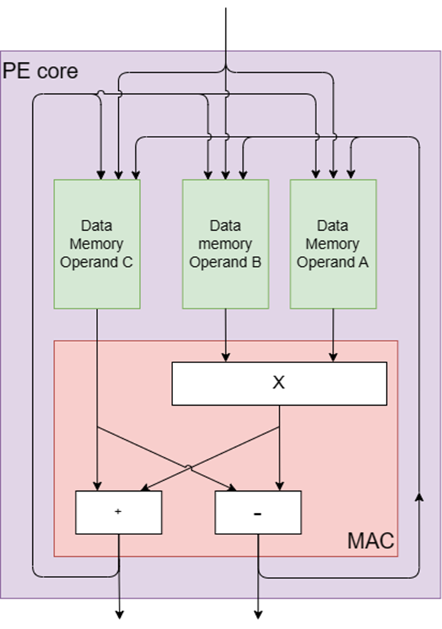
Figure 2: PE Core Components
PE bit width
PE natively supports large-word module arithmetic operations (up to 256-bit words). The trade-off between high-bit-width native support and low-bit-width native support in PE stems from the need to balance the efficiencies of different operand sizes.
When a PE has high-bitwidth native support, it is optimized for handling large operand sizes without breaking them into smaller chunks. However, this optimization comes at the cost of less efficient operations on smaller bitwidths because PEs are underutilized. On the other hand, when a PE has low-bit-width native support, it is optimized to handle small operand sizes more efficiently. However, this optimization leads to inefficiencies when dealing with larger bit-width operations, since the PE needs to break up larger operands into smaller chunks and process these chunks sequentially.
The challenge is to find the right balance between high and low bitwidth native support to ensure efficient processing across a wide range of operand sizes. This balance should consider common bit widths prevalent in the target application domain (i.e., ZK protocols), and weigh the pros and cons of each design choice. In the case of the ZPU architecture, a word size of 256 bits was chosen as a good balance.
PE connection
All PEs are connected in a ring, and each PE is directly connected to two adjacent PEs to form a ring network. This ring connection allows control data to travel efficiently between different PEs. PEs are also connected by interconnect components, a barrel shifter-like mechanism that enables direct connections between different PEs over time. This setup allows a PE to send and receive information from all other PEs.
peripheral components
The architecture also integrates off-chip High Bandwidth Memory (HBM) to support high memory capacity and high memory bandwidth. Multiple PEs are gathered together to form a PE cluster, and each PE cluster is connected to an HBM bank or channel. Additionally, an ARM-based on-chip CPU subsystem is included to manage overall system operations.
Grade
To evaluate the performance of the ZPU, we consider key operations of the algorithms we aim to accelerate. We mainly study NTT butterfly operation and elliptic curve (EC) point addition operation. To evaluate the total computation time of MSM and NTT operations, we calculated the total amount of computation instructions they require and divided them by the clock frequency and the number of PEs.
The NTT butterfly operation is performed every clock cycle. For the key element elliptic curve point addition operation in multiscalar multiply (MSM), we deconstruct it into basic machine-level instructions that can be executed on a single PE. We then calculate the number of clock cycles required to complete this operation. Through analysis, we determined that each elliptic curve point addition operation can be performed every 18 clock cycles.
These assumptions provide the basis for our performance estimates and can be adjusted as needed to reflect different algorithmic requirements or hardware capabilities.
According to our calculations, a configuration of 72 PEs running at the GPU's 1.305 GHz frequency is sufficient to match the performance of the GPU category winner in Zprize 's MSM operation. Both Yrrid Software and Matter Labs achieved this feat, achieving a result of 2.52 seconds per 4 MSM calculations using an A40 NVIDIA GPU. The comparison is based on a fixed-base-point MSM calculation involving 2²⁶ scalars randomly selected from the BLS 12-377 scalar field, and a fixed set of elliptic curve points from the BLS 12-377 G1 curve and a finite set of randomly sampled input vectors from the scalar field element.
Based on our PE area estimates, an ASIC using the 8nm process, the same process technology used in the A40 GPU, can accommodate approximately 925 PEs in the same 628 mm2 area as the A40 GPU. This means we achieve about 13x higher efficiency than the A40 GPU.
PipeZK is an efficient pipeline accelerator designed to improve the performance of Zero-knowledge Proof(ZKP) generation, with dedicated MSM and NTT cores that optimize the processing of multi-scalar multiplications and large polynomial computations, respectively.
Compared to PipeZK, we found that a configuration of only 17 PEs running at PipeZK's frequency of 300 MHz is sufficient to match PipeZK's MSM operation performance. PipeZK performs an MSM operation at 300 MHz on a 2²⁰ length MSM in the BN128 curve, taking 0.061 seconds to complete. Furthermore, to match the performance of PipeZK's NTT operation, which takes 0.011 seconds to run a 2²⁰-element NTT of 256-bit elements at 300MHz, we need about 4 PEs running at the same frequency. Overall, to match the performance of PipeZK running both MSM and NTT, we need 21 PEs.
Based on our area estimates, an ASIC using a 28nm process (the same process technology used in PipeZK) can accommodate approximately 16 PEs in the same 50.75 mm2 area as the PipeZK chip. This means we are slightly less efficient than PipeZK's fixed architecture (25% less efficient), while still being fully flexible to adapt to different elliptic curve and ZK protocols.
The Ring Processing Unit (RPU) is a recent effort to accelerate the computation of ring-based learning with error (RLWE), which is the basis of various security and privacy-enhancing techniques, such as homomorphic encryption and post-quantum encryption.
Compared to the RPU, our calculations show that to match the performance of the RPU at the optimal configuration (128 banks and HPLEs) when computing 64K NTT for 128-bit elements, we would need about 23 PEs at the RPU's 1.68GHz frequency run on. Our analysis shows that an ASIC using the same 12nm process technology as the RPU can accommodate approximately 19.65 PEs within the 20.5 mm² area occupied by the RPU. This means we are slightly less efficient than RPUs (15% less efficient), while being compatible with primitives other than NTT.
TREBUCHET is a Fully Homomorphic Encryption (FHE) accelerator that uses a Ring Processing Unit (RPU) as an on-chip block. Slices also facilitate memory management by scheduling data close to compute elements. RPUs are replicated throughout the device, enabling software to minimize data movement and take advantage of data-level parallelism.
Both TREBUCHET and ZPU are based on the ISA architecture and large arithmetic word engines that support very long words (128 bits or higher) under modular arithmetic. However, the added value of the ZPU compared to an RPU or TREBUCHET SoC is that it expands the set of problems that the architecture is designed to solve. RPU and TREBUCHET mainly focus on NTT, while ZPU supports more primitives such as multiscalar multiplication (MSM) and arithmetic-oriented hash functions.
Summarize
Our performance evaluations show that the ZPU can match or even exceed the performance of existing state-of-the-art ASIC designs, while providing greater adaptability to changes in the ZK algorithm and cryptographic primitives. While there are tradeoffs to consider, such as the balance between high and low bitwidth support in PEs, the design of the ZPU is carefully optimized to ensure efficient processing across a wide range of operand sizes. For those interested in learning more about ZPU or exploring potential collaborations, please feel free to contact us. We look forward to sharing more updates on the progress and future development of the ZPU project with you.
Thanks to Weikeng Chen for the review.